Japan’s government-backed chip venture Rapidus has fallen behind schedule on its pledge to mass-produce 2-nanometre semiconductors by March 2028, with engineers yet to produce functioning SRAM cells, a critical milestone that needed to be cleared by summer, according to people familiar with the matter cited by The Japan Times.
The Missing Tool
The delay puts a sharper focus on a question that has dogged the project since its inception: whether Rapidus can reach 2-nm volume without guaranteed access to ASML’s High-NA EUV lithography systems. The Dutch firm’s Twinscan EXE platforms are the only tools capable of printing the finest features of a 2-nm logic process in a single exposure. Without them, chipmakers must rely on multi-patterning with existing Low-NA EUV machines, a workaround that adds cost, complexity and cycle time — precisely the variables Rapidus has pledged to shrink.
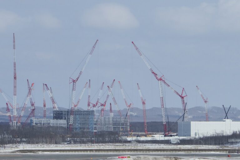
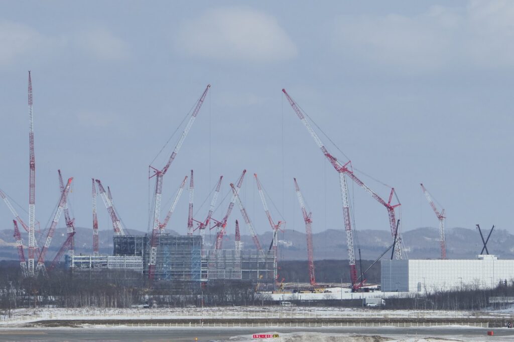
Rapidus was established in August 2022 with the backing of eight Japanese majors — Denso, Kioxia, MUFG Bank, NEC, NTT, SoftBank, Sony and Toyota — aiming to restore a domestic leading-edge capability that has largely vanished since Elpida Memory’s collapse in 2012. The company’s Chitose, Hokkaido pilot line is sized for 25,000 wafers a month, a fraction of the scale operated by incumbents.
Supply Chain Reality
ASML has a multi-year backlog for High-NA systems. Intel received the first production unit in late 2023; TSMC and Samsung followed with early installations for development. Rapidus, a new entrant with no revenue, sits further down the queue. The company has not publicly confirmed a delivery slot for a High-NA tool. Until one arrives in Chitose, its engineers are developing the 2-nm process on Low-NA equipment, either at the pilot line or through its partnership with IBM at the Albany NanoTech Complex in New York, where IBM operates an ASML High-NA scanner for research.
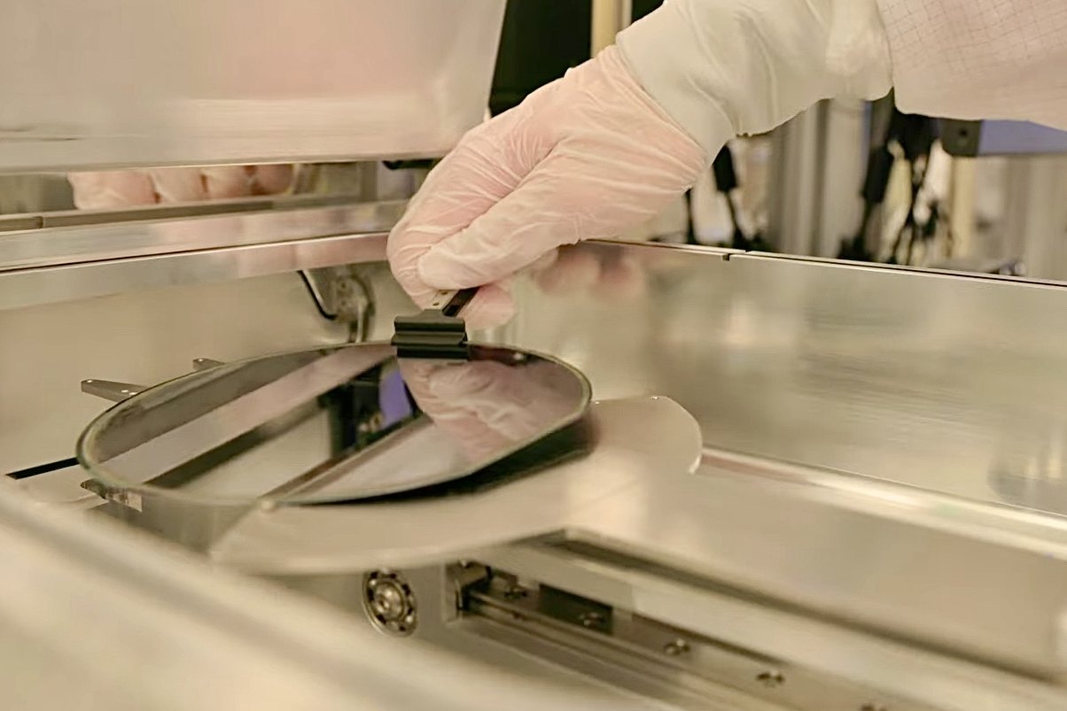
That IBM link is operational, not just ceremonial. IBM Japan opened a dedicated support base in Chitose on November 6, a 20-minute drive from the Rapidus site, to provide manufacturing execution and quality systems ahead of the planned mass-production start in the second half of fiscal 2027. Rapidus has adopted core semiconductor manufacturing systems from IBM Japan, and engineers have been hosted at IBM’s US facilities. “When we think about mass production, physical proximity is reassuring,” Rapidus Senior Managing Executive Officer Shigehiro Fujino said at the opening.
Design Bandwidth
While the fab waits for lithography, Rapidus is trying to accelerate the front end. On October 26, the company inaugurated two HCLTech engineering centres in Bengaluru and Hubli, India, focused on mask design, process design kit development, design-technology co-optimisation and layout. Jiji Press reported the centres began full operation immediately. HCLTech will also train chip design experts for Rapidus’s future staffing needs in Japan. The partnership addresses a bottleneck: chips start with design rules and layout work, and that work requires thousands of trained engineers.
The Scale Gap
The numbers illustrate the mountain Rapidus must climb. Terafab, the semiconductor project backed by Tesla and SpaceX, has told Japanese equipment makers it targets 1 million wafers a month from 2032 — roughly 40 times Rapidus’s planned pilot-line capacity and about 70 per cent of TSMC’s total 2025 output of more than 17 million 12-inch-equivalent wafers a year, according to Nikkei. Terafab is targeting mass production in the second half of 2028, with some equipment delivery deadlines only months away. “Right now, the biggest topic in the semiconductor industry isn’t Kioxia or Rapidus. It’s Elon Musk,” a supplier executive told Nikkei.
Rapidus’s stated goal remains a 2-nm process by 2027. The failure to produce working SRAM cells by summer means the company is at least months behind that schedule. The next concrete marker is whether a High-NA EUV tool arrives in Chitose in time to validate the process window for the March 2028 deadline.
Sources
- Rapidus
- Japan’s Rapidus is said likely to miss mass production deadline
- Rapidus HCLTech Open 2 India Chip Centers [2026]
- IBM Japan Opens Rapidus Support Base in Chitose, Answering Mass-Production Push with Proximity — BigGo Finance
- Musk's Terafab tells Japanese toolmakers it wants 1 million wafers a month from 2032, Nikkei reports
- TSLA Stock Slips Overnight As Cybertruck Makes Way For Cybercab — Terafab Reportedly Eyes 1M Wafers Monthly
Photo: どういたしまして (CC BY-SA 4.0)